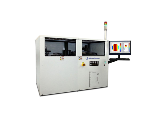
The UltraMap 200-BP Wafer measurement system precisely measures wafer thickness, flatness and shape using MicroSense's patented non-contact auto-probe back pressure technology. The UltraMap 200-BP is an extremely flexible system since it can measure a wide range of wafer thicknesses and any wafer material. Wafer surface finish has no effect on the measurement - the UltraMap BP-200 measures as sawn, lapped or polished wafers.
0.5 micron absolute thickness measurement accuracy on wafers with <500 micron bow
1.5 micron absolute thickness accuracy on wafers with >500 micron and <1000 micron bow
Auto calibration of back pressure sensors with integrated calibration standards - no need for master wafers
High repeatability, non-contact air bearing stage for repeatable wafer positioning